
|
University of Southampton Institute of Transducer Technology |
Micromachined Silicon Capacitive Sensors |
Introduction
USITT has developed a micromachined silicon capacitive absolute pressure sensor designed for industrial applications. Capacitive pressure sensors rely upon the applied pressure altering the distance between the two electrodes resulting in a change in the capacitance. Typically, the position of one electrode is fixed whilst the second electrode moves relative to it. Many capacitive based microsensors have been developed to date but continuing advances in process technologies offer new opportunities for fabricating such devices. Silicon fusion bonding, improved silicon etching processes and the use of finite element modelling have enabled the rapid development of recent devices. The aim of this work was to develop a working prototype exhibiting a large change in capacitance over the desired pressure range (0-8 bar), operating behaviour that simplifies linearisation, and can be fabricated using low-cost silicon batch fabrication processes.
Sensor Design
The device presented here consists of two silicon substrates fusion bonded together with a silicon dioxide (SiO2) passivating layer sandwiched between them (see fig. 1). The silicon wafers form both the mechanical sensor and capacitor electrodes and therefore no metalised electrodes are required. The top silicon substrate has been etched to form corrugations in the diaphragm to define the behaviour of the diaphragm under pressure. The thickness of the SiO2 layer determines the gap between the electrodes and therefore, along with the bonded circumference around the diaphragm, the base capacitance of the device. Both free surfaces of the bonded wafer pair are coated with 1mm aluminium enabling the top contact to be formed by wire bonding to the top surface, the bottom by bonding the chip to the sensor package with conductive epoxy.
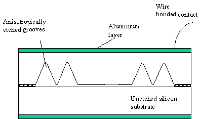
Figure 1 – Schematic of capacitive pressure sensor.
Finite Element Analysis
Capacitive pressure sensors are inherently non-linear since the capacitance, C, is inversely proportional to the distance between the electrodes. This non-linear behaviour is further exacerbated by the bending of the diaphragm under pressure. In order to reduce this effect, finite element analysis (FEA) has been used to design the diaphragm so that the degree of bending across the top electrode is greatly reduced. Figure 2 shows FEA calculated deflection of the corrugated diaphragm compared to a basic anisotropically etched diaphragm. The dimensions of the corrugated diaphragm are shown in figure 3 and a FEA plot displaying the FE mesh is shown in figure 4. FEA was used to simulate changes in the above dimensions in order to achieve a suitable level of sensitivity over a design pressure range of 0-8 bar. Modifying the dimensions can also simulate other pressure ranges.
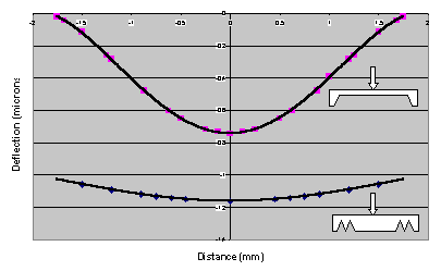
Figure 2 – Graph plot of deflection along top electrode for 2 bar applied pressure (the centre of the diaphragm is at 0mm, the edge 1.5mm)
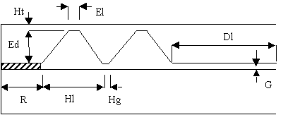
Figure 3 – Cross-section of half sensor chip, Ht=200, El=200, Ed=100, R=750, Hl=800, Hg=100, Dl=1500, G=2 (all dimensions in microns).
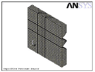
Figure 4 – FEA element plot of one quarter of device.
Device Fabrication
The sensors have been fabricated using double polished (100) silicon wafers, 100mm diameter, 525 mm thickness with a resistivity of 0.1 ohm-cm. The fabrication process involves double-sided photolithography, KOH etching, fusion bonding and metalisation. The process has been developed so that just two masks are required, plus one thick-film printing screen. The first mask patterns what will be the top surface of the silicon diaphragm. This defines the double-sided alignment features and chip frame. These were etched into the silicon to a depth of 2 mm using a standard SF6 plasma etch using a resist mask. The resist was stripped and 600 nm wet oxide grown and 160 nm silicon nitride deposited using Low Pressure Chemical Vapour Deposition (LPCVD Si3N4).
The second mask contains the double-sided alignment feature corresponding to that etched into the front surface and the pattern required to successfully etch the diaphragm corrugations in KOH. The double-sided alignment ensures the diaphragms are correctly located within the chip frames enabling accurate sawing of the wafers at the end of the process. The convex corners in the design have been protected using standard compensation features [8]. The patterns are first etched through the oxide and nitride passivation layers using a standard CHF3 and Ar plasma etch. The wafers were then dip etched in 20:1 Buffered Hydroflouric acid (BHF) before immersing the wafers in KOH solution (44g crystals to 100ml de-ionised water) and heated to 70oC for 12 hours. The solution is continually agitated providing an even etch rate across the wafers and an improved surface finish. The nitride and oxide layers were then stripped after which 2 mm oxide were grown on the wafers in a wet oxidising furnace at 1100oC. It is this oxide thickness that determines the height of the gap between the two electrodes, but in order to form the gap the oxide must be removed from the area forming the top electrode. Standard photolithography could not be used to pattern the oxide layer due to the surface topology of the wafer preventing the resist from being evenly spun onto the wafer. This problem was overcome by thick-film printing a polymer ink through a patterned screen onto the backs of the wafer. A 40 mm thick layer of Ronascreen OPSR 5100 series soldermask, was printed onto the wafer and cured at 140oC for 10 minutes. The wafers were then immersed in 7:1 BHF until hydrophobic. This simultaneously removed the oxide from the top surface of the wafer where the subsequent metal was to be evaporated. The thick-film mask was then removed with an oxygen plasma.
The wafers were then prepared for bonding using a standard RCA clean. In this instance, the wafers were joined in air, but oxygen could be used to achieve a higher quality vacuum. The pre-bonded wafer pairs were then heated up to 1100oC in nitrogen to achieve the full strength fusion bond. Finally, the wafers were dip etched in BHF, 1mm aluminium e-beam evaporated onto both exposed surfaces and the wafers sawn into individual die. A photograph of the cross section of a completed device is shown in figure 5.
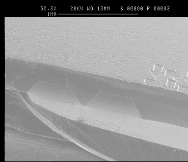
Figure 5 – SEM photograph showing cross-section of bonded sensor die.
Results
The sensors have been designed for sensing pressures up to 8 bar, after which the two electrodes touch. Several devices have been packaged as shown in figure 7 and pressure tested on a Barnett dead-weight tester using a Keithley 200 impedance meter. The capacitance/pressure relationship is characterised by equation 1, where Cb is the base capacitance, P pressure and k1 and k2 constants specific to each sensor.
|
(1) |
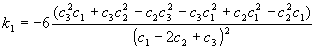
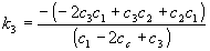
Measuring the capacitance values, c1, c2 and c3, at 1, 4 and 7 bar and applying equations 2 to 4 the values for k1, k2 and Cb can be calculated for each sensor.
|
(2) |
|
(3) |
|
(4) |
Linearisation of the sensor output is achieved via a simple algorithm stored in a microcontroller. A PIC16C55 manufactured by Amina Micochip was chosen for this purpose. This is preferable to a look up table which requires interpolation between stored values. The base capacitance is approximately 1 nF and the change in capacitance over the 8 bar pressure range is in excess of 100 pF providing a large and robust signal. Figure 6 shows the output of the linearising algorithm, this being obtained using measured values of capacitance vs. pressure. The small error visible is due to the inaccuracy of the capacitance meter used to measure the sensor during the pressure tests.
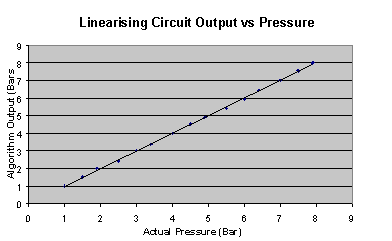
Figure 6 – Calculated sensor output versus actual pressure.
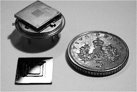
Figure 7 – Photograph of packaged device and etched diaphragm.
Conclusions
The device presented here is capable of being manufactured using standard batch fabrication techniques where large numbers of wafers are processed simultaneously. The design exploits the mechanical properties of silicon resulting in a repeatable device that will not yield or suffer fatigue failure. With careful packaging, the long-term drift potential of the sensor chip is excellent. The device is very rugged and can withstand very large overpressures since the bottom electrode acts as a deflection stop limiting the movement of the diaphragm. The sensor output is in excess of 100 pF over the 8 bar pressure range providing a robust signal. Currently, the bonding process is being improved in order to reduce the bonded area required around the sensor thereby reducing base capacitance and increasing chip density on the wafer. Future work includes incorporating electronics on the actual sensor chip.
|
![[Uni. Home]](images/unilogo.gif)