
|
University of Southampton Institute of Transducer Technology |
Combined Thick-film/Silicon Micromachined Structures |
Intoduction
Many silicon micromachining processes have been developed for the fabrication of a wide range of MicroElectroMechancial (MEMS) devices. A recent development has been the deposition of thick film lead zirconate titanate (PZT) layers on silicon using standard screen printing techniques resulting in PZT layers in excess of 100mm thick. This thickness of PZT is capable of relatively large actuating forces when compared to piezoelectric thin films deposited using sputtering or sol-gel techniques, and other actuating mechanisms.
One difficulty associated with the thick film printing process is the pressure applied to the substrate during the printing process. The mechanical structure upon which the PZT is to be printed must be of sufficient strength to withstand this pressure. Another limitation of the thick film process is the accuracy of registration of the printed layers with respect to micromachined structures and layers patterned using standard photolithographical techniques. The registration accuracy of thick film layers printed using typical processing equipment is +/- 50mm, although printers using optical alignment techniques will improve on this.
Both of these restrictions can be overcome if the thick film printing processes are carried out first followed by the silicon micromachining. This results in the printing steps being carried out on an unetched silicon wafer. The subsequent micromachining processes could, where applicable, be aligned to the printed layer thereby improving registration. Such an order of processing however introduces many potential difficulties.
We have completed a comprehensive investigation into the compatibility issues of micromachining silicon wafers with PZT layers printed on the surface. It assesses the effect of many standard micromachining processes employed at the Southampton University Microelectronics Centre (SUMC) upon the printed PZT layer. In particular the adhesion of the printed layer to the substrate and its internal structure have been studied after exposure to each micromachining process.
Thick Film Printed PZT Technology
The printed PZT layer is sandwiched between two electrodes thereby forming a capacitor structure. A typical layout is shown in figure 1. The optimum bottom electrode material has been identified as a 500nm Pt film with a 50nm Ti intermediate adhesion layer. A 0.5 to 1mm thick thermal silicon dioxide (SiO2) passivation layer was first grown on half the substrates, the other half remaining unpassivated. The bottom layer electrode was patterned as shown in figure 1 using standard contact photolithography and ion beam milling. In this manner a wide range of finely dimensioned electrode patterns can be simply formed on the silicon substrate. Alignment aids were also patterned onto the substrate to assist registration of the subsequent printed layer to the Pt electrode. Th top electrode can be formed by screen printing a conductive layer or also by evaporating Al thin films.
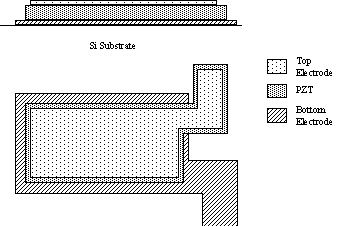
Figure 1 – PZT/electrode structure
The PZT paste was made from 95% PZT-5H powder, 6mm average grain size, 5% lead borosilicate powder and 5ml ESL 400 organic vehicle and this paste can be printed through a stainless steel screen. Typically two print strokes are carried out after which the ink is dried at 140oC and then fired in air at between 850 and 950oC. An additional double print, dry and fire yields PZT thickness of up to 100mm. For the purposes of this study a single two stroke print run was used yielding a fired film thickness of between 50 and 60 mm. After firing, a reaction occurs between the silicon and the PZT resulting in the formation of material around the PZT. This is characterised by reaction sites as shown in figure 2 which can inhibit sunsequent micromachining processes. An SEM photo of the cross-section of the fired ink is shown in figure 3.
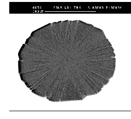
Figure 2 – PZT reaction site
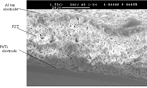
Figure 3
Micromachining of Printed Wafers
After printing PZT onto silicon substrates a number of typical micromachining etches have been evaluated. The suitability of these processes has been reviewed according to their effect on the PZT, the patterned bottom electrode, the adhesion of the fired assembly to the substrate and the relative dielectric constant of the PZT. For the purpose of this study the PZT has been printed directly onto unpassivated silicon wafers, wafers with 1mm thermal oxide, Pt electrodes on unpassivated silicon and Pt electrodes on 1mm thermal oxide. Top electrodes have not been incorporated in this part of the study since the effects of these etches on aluminium is well documented.
In each case the substrate was exposed to the etch for a suitable period of time. The effect of the etch was then evaluated by a series of simple tests. The adhesion of the electrode / PZT structure to the substrate was monitored by performing a standard thick film tape test in which adhesive tape is stuck to the PZT and then pulled away. The adhesion of both the bottom electrode to the substrate and the PZT to the electrode was checked in this manner. Also the tape can be visually checked to see if the sintering and binding of the PZT layer has been affected by the etch. This would be evidenced by PZT particles remaining stuck to the tape having been pulled away from the remainder of the material.
The height of the PZT was measured before and after the etch using a Tencor Instruments Alpha Step Probe to determine if etching had occurred. The continuity of the bottom electrode was checked by measuring the resistance across its length and by observing samples in the SEM. The relative dielectric constant, er, of the PZT after etching was measured by measuring the capacitance across the PZT using a probe with a known surface area.
The etched substrates were compared to reference samples printed and fired simultaneously as part of the same batch. The reference samples were prepared on the same types of substrates as those used in the etch tests. The properties of the PZT thick film and Pt bottom electrode for reference samples from groups A to D are as follows:
PZT thickness = 51 - 58 mm
Dielectric constant = 390 - 450
Electrode resistivity = <0.01 ohms.cm
Electrode adhesion = 100%
PZT adhesion = 100%
Wet Processes
Wet processes include various etching and cleaning solutions used in liquid form and are of considerable interest when micromachining silicon. Established silicon etches, e.g. potassium hydroxide (KOH) and tetramethyl ammonium hydroxide (TMAH), combined with techniques such as the boron etch stop provide a means of removing large amounts of silicon from wafers whilst simultaneously defining complex structures. Wet etches are also used to strip or pattern different material layers such as silicon dioxide, silicon nitride and various metals. Fuming nitric acid is a standard wet chemical commonly used in micromachining batches to clean wafers and strip resist. After wet processing wafers are rinsed and dried in some manner. In this study the samples have been rinsed in de-ionised water for 10 minutes and then spun dry. Wet etches will be of particular interest given the porous nature of the PZT film.
Plasma Etching of PZT
Plasma processes are widely used in the fabrication of both microelectronic and micromechanical devices. The plasma processing of interest to this study is the etching of PZT, Pt, Si and SiO2 material. Plasma etching is typically a combination of physical and chemical processes. Chemical processes weaken atomic bonds whilst ion bombardment physically sputters material away. The nature of the plasma and its reactivity with the material, and the power driving the ion bombardment, are key parameters in determining the effect of the etch. The aim of this part of the study was to assess the effect of standard plasma etches for SiO2, Si3N4 and Si on the PZT/Pt structure. This will enable the identification of etches useful for micromachining that do not effect the PZT/Pt.
Summary of Results
The suitability of each etch is summarised in table 1. The etched silicon surface is shown in figure 4 where the effect of the reaction sites leaves clearly visible unetched features.
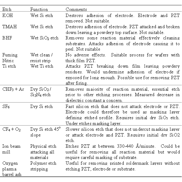
Table 1 - Summary information of etch processes
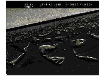
Figure 5 - SEM photograph of SF6 etched substrate
Contact: usitt@soton.ac.uk
© 2002 USITT & Department of Electronics and Computer Science
![[Uni. Home]](images/unilogo.gif)