|
University of Southampton Institute of Transducer Technology |
Thick-film Elastic Wave Sensors |
This project relates to acoustic wave sensors fabricated by a standard thick-film deposition process and using a lead zirconate titanate (PZT) piezoelectric paste developed within the group. An investigation of the paste to maximise the piezoelectric charge coefficients was undertaken, and in addition the optimal electrode material and configuration was investigated. This part of the programme led to the development of a dedicated test rig for measuring the piezoelectric properties of thick-film piezoelectrics on alumina. It quickly became apparent that the paste itself would have a variety of applications in the field of silicon micromachining, and the technique was migrated onto silicon where its use as an actuator has been established.
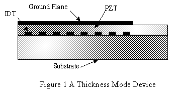
Preliminary work indicated that interdigitated electrodes (IDTs) were suitable for launching acoustic waves on alumina. This work was extended in the project and the nature of the waves generated by two types of IDT structure was investigated. Although in principle IDT electrodes on alumina look similar to the IDTs used in Surface Acoustic Wave (SAW) devices, the physics of elastic waves on alumina is complicated by fact that the thickness of common alumina substrates is comparable with the wavelength of the acoustic signal (typical thickness is around 630 m m). The consequence of this is that a true ‘surface’ wave is not launched. The type of wave is more closely related to a plate (or Lamb) wave. Plate waves are dispersive and their associated wave equations require numerical solution. Predictions of the resonant frequency of these devices required a mathematical model that was implemented on the software package Matlab. The presence of the PZT layer on the transducer further complicated matters. By use of the Matlab model and various experimental designs of thickness mode type transducers it became possible to implement an asynchronous Lamb wave device with known frequency response.
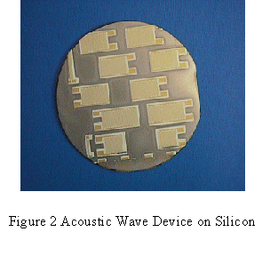
It became apparent that being able to print PZT onto silicon would have many attractions in the field of Micro-ElectroMechanical Structures (MEMS), in particular solid-state actuators. Investigations showed that the PZT paste could be printed onto passivated silicon (i.e. silicon dioxide and silicon nitride layers) but the lead evaporated out of the layer and condensed on the surface of the silicon thereby creating conductive paths. In addition, the presence of the PZT caused reactions with the gold electrode layers. The platinum electrode layers, however, were very successful and by careful design it is now possible to produce devices with significant piezoelectric activity. IDT patterns were also printed onto silicon wafers to see if the generation of acoustic waves was possible (figure 2). Acoustic waves can be generated on silicon but care must be taken to transmit parallel with the crystal structure to ensure a constant acoustic velocity. There is potential for developing this technology on silicon as micromachining techniques allow the fabrication of arbitrary diaphragm thickness.