Zepler Institute Cleanroom Facilities
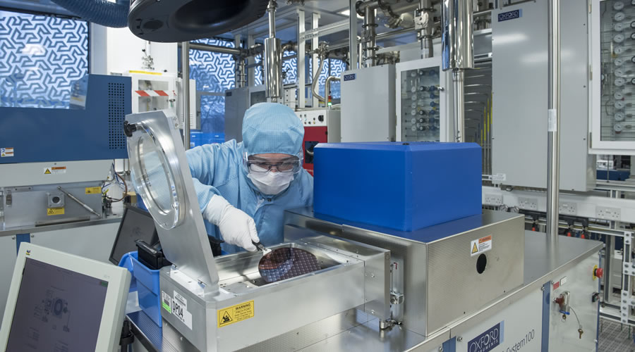
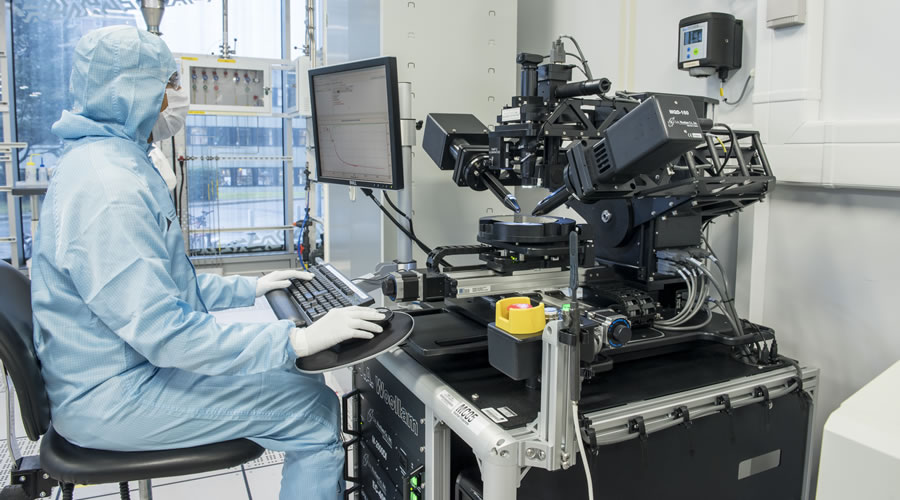
The Cleanroom is the largest multidisciplinary cleanroom of its type in the UK offering world-class facilities and expertise in nanoelectronics, optoelectronics, quantum technologies, device physics and biotechnology. We take new nanotechnology concepts and realise them into prototypes for the next generation microprocessors, broadband internet system, bio-medical and environmental sensors.
Teaching
Our undergraduate and MSc students are taught by academic cleanroom users, who are expert in their research field. Students will learn from the academics on their latest scientific findings originated from the Cleanroom activities. Our students will have the opportunity to select specialisation modules such as Microfabrication and Bionanotechnology that have cleanroom lab work as part of their learning experiences.
Facilities and equipment
The Zepler Institute Cleanroom Facilities consist of:
- Southampton Nanofabrication Centre (Advanced research cleanroom for novel electronic and optoelectronic devices)
- Teaching and Research Cleanroom (UG and MSc teaching; early fabrication training centre for PhDs and device prototyping)
- Integrated Photonics Cleanroom (Cleanroom for processing novel optical materials for photonic devices)
- Silica Fibre Lab (Advanced optical fibre drawing towers and processing facility)
- Novel and Compound Glass Lab (Research in novel chalcogenide glasses and two dimensional materials)
- Flame Hydrolysis Deposition Lab (Specialised in direct deposition of various optical grade materials for photonic circuits)
- Focused Ion Beam Lab (Fast prototyping lab for metamaterials research)
- Stepper Lithography Cleanroom (Advanced optical lithography suite for wafer scale silicon photonics and electronics)
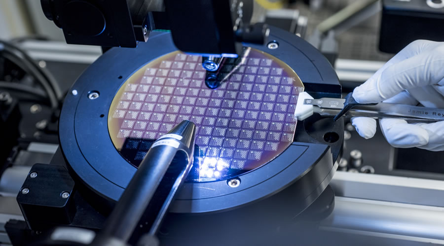
We have state-of-the-art fabrication equipment from making the smallest of transistors at 10 nanometre to drawing tens of kilometre of optical fibre cable. Two key tools are:
- Electron Beam Lithography System at the Southampton Nanofabrication Centre: A research tool used for direct write circuit patterns onto semiconductor wafers capable of delivering less than 5 nanometre feature size for nanoelectronic and photonic device applications.
- Optical Fibre Drawing Tower at the Silica Fibre Lab: A specialised tool for the manufacturing of cutting edge fibre optics for the next generation broadband network infrastructure.
Research
The Zepler Institute's unique multidisciplinary environment enables over 300 researchers to focus on developing the cutting-edge technologies required for the 21st century. The Institute works across six major research areas: Electronics and Electrical Engineering; Fibres and Lasers; Nanoelectronics and Nanotechnology; Nanophotonics and Metamaterials; Photonics Systems, Circuits and Sensors; and Quantum Light and Matter.
Business and Enterprise
We are open to discussing business opportunities with industrial and academic partners on how we can assist them to pursue their interests, either by providing commercial fabrication services or collaborative research project. Companies can make enquiry through our Zepler Institute Business Development Unit and ECS Partners Ltd for consultancy work.